A fluke discovery could pave the way towards improved graphene-based electronics
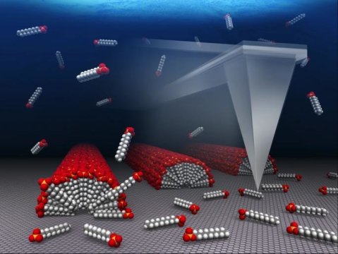
A group of scientists at Nagoya University have developed a simple and powerful method to construct perfectly unidirectional molecular assembly structures on graphenes, according to a study reported in the journal Scientific Reports. Discovered accidentally during other research, the method relies on a common laboratory tool, atomic force microscopy (AFM), to control molecular alignment.
Graphene, which are sheets made out of carbon, is attracting wide interest from many scientists as a powerful candidate for the next generation of electronics materials due to their unique properties. The development of a reliable method that enables the perfect alignment of molecules or molecular assemblies on a graphene surface may lead the way to tune the electric properties of graphene, and to improve the performance of graphene-based electronic devices. Although widely studied in recent years, the growth of well-aligned molecular nanostructures exclusively along a desired direction is still difficult. This is because the graphene surface has three-fold symmetry, which are thermodynamically equivalent to each other, thus making it difficult to align the molecules in an oriented direction.
To resolve this problem, a team led by Dr. Yuhei Miyauchi and Professor Kenichiro Itami of the JST-ERATO Itami Molecular Nanocarbon Project and the Institute of Transformative Bio-Molecules (ITbM), focused on the physical changes induced by AFM tip scanning. AFM, a technique mainly used for analyzing surfaces, produces images showing the surface unevenness of samples by sliding a probe tip over the surface area. The team suspected that tip scanning modifies the thermodynamical conditions on the graphene surface and affects the direction of molecular alignment.
The team investigated how AFM tip scanning leads to changes in molecular alignment on the graphene surface. They used sodium dodecyl sulfate (SDS), a common surfactant molecule, as a model molecule. Studies have shown that SDS forms ribbon-like assembles on the graphene surface.
Using a microsyringe pump, the SDS solution was slowly injected into a multilayer of graphene in a water droplet. The team compared how the SDS molecules adhered to the graphene, a process called adsorption (not be confused with absorption), with and without AFM tip scanning.
An AFM height image recorded 1 hour after SDS injection showed random unevenness on the surface, which indicates random adsorption of SDS molecules on the graphene surface. After 15 minutes of intense AFM scanning, the SDS adsorption morphology drastically changed and many ribbon-like molecules were observed. This phenomenon indicated that the strength and direction of AFM tip scanning affects the orientation of the generated SDS ribbons.
“We discovered this phenomenon accidentally when we were carrying out another research project,” says Dr. Liu Hong, a postdoctoral researcher who mainly conducted the experiments. “We noticed that looking at the images of AFM, the SDS ribbon grew in the same oriented direction by AFM tip scanning.”
“We genuinely wanted to clarify this surprising phenomena,” says Yuhei Miyauchi, a group leader of the JST-ERATO project.
The team analyzed the correlation between the AFM scanning direction and the observed ribbon orientation. They discovered that the SDS ribbons grew easily when the relative angle between the ribbon growing axis and the scan direction is larger. In addition, computational calculations suggested that adsorbed SDS molecules are actually removed when they are forced to rotate under the AFM scanning conditions. Adsorbed SDS molecules with a relatively large angle to the AFM tip scan direction are rotated and are easily removed. Therefore, the molecules adsorbed with small angles to the AFM tip scan direction act as the nuclei and grow to become the SDS ribbon.
On the basis of their understandings, the team tried to construct perfectly aligned SDS molecular assemblies on graphene.
“The most difficult part of this research was how to control the growth and direction of SDS ribbons with precision,” says Hong. “Once the SDS ribbons were grown, their orientations did not change under the AFM scanning conditions. We had to perform rapid AFM scans in time just after that very moment where SDS molecules are injected into the water on the graphene surface.”
Under finely tuned AFM scanning conditions, they succeeded in constructing individual one-dimensional molecular assemblies, which are aligned along a selected symmetry axis of the graphene lattice.
“In AFM analysis, the dynamical mechanical effects to the sample by AFM tip scanning have been considered to be unfavorable,” says Dr. Taishi Nishihara, a postdoctoral researcher who conducted the statistical analyses and analyzed the mechanism of this experiment. “Our findings on the hidden usefulness of the effects induced by AFM tip scanning may also provide insight to other researchers in various related fields.”
“The best part of this research is that we were able to show that the AFM scan can induce the ‘symmetry breaking’ effect of the molecular pattern on graphene,” says Hong. “It can be very important for the growth of anisotropic molecular patterns on two-dimensional (2D) materials, such as super lattices, which are now essential in both academic and industrial research.”
“Our concept of breaking the surface symmetry can be applicable for various purposes such as generating molecular circuits in molecular electronics and controlling cell chemotaxis in bioscience,” says Miyauchi.
“We hope that our discovery will lead to a distinctive breakthrough in not only chemistry but in related fields that involve molecular nanostructures and their alignment,” says Itami, the director of the JST-ERATO project and center director of ITbM.
Source: Science Daily












Leave a Comment
You must be logged in to post a comment.