Empa researchers, together with colleagues from the Max Planck Institute for Polymer Research in Mainz and other partners, have achieved a breakthrough that could eventually be used for precise nanotransistors or, in the distant future, possibly even quantum computers, as the team reports in the current issue of the scientific journal Nature.
A material that consists of atoms of a single element, but which has completely different properties depending on the atomic arrangement may sound strange, but is this is actually the case with graphene nanoribbons. The ribbons, which are only a few carbon atoms wide and exactly one atom thick, have very different electronic properties depending on their shape and width—they can be conductors, semiconductors or insulators. An international research team led by Empa’s nanotech@surfaces laboratory has now succeeded in precisely adjusting the properties of the ribbons by specifically varying their shape. Not only can these three usual electronic properties be varied; the method can also be used to generate specific local quantum states.
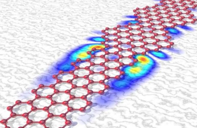
So what’s behind it? If the width of a narrow graphene nanoribbon changes, in this case from seven to nine atoms, a special zone is created at the transition. Because the electronic properties of the two areas differ in a special, so-called topological way, a “protected” and thus very robust new quantum state is created in the transition zone. This local electronic quantum state can now be used as a basic component to produce tailor-made semiconductors, metals or insulators – and possibly even as a component in quantum computers.
The Empa researchers under the lead of Oliver Gröning were able to show that if these ribbons are built with regularly alternating zones of different widths, a chain of interlinked quantum states with its own electronic structure is created by the numerous transitions. The exciting thing is that the electronic properties of the chain change depending on the width of the segments. This allows them to be finely adjusted – from conductors to semiconductors with different bandgaps. This principle can be applied to many different types of transition zones – for instance, from seven to eleven atoms.
“The importance of this development is also underlined by the fact that a research group at the University of California, Berkeley, came to similar results independently of us,” said Gröning. The work of the U.S. research team has been published alongside Gröning’s in the same issue of Nature.

On the way to nanoelectronics
Based on these novel quantum chains, precise nano-transistors could be manufactured in the future – a fundamental step on the way to nanoelectronics. Whether the switching distance between the “1” state and the “0” state of the nanotransistor is actually large enough depends on the bandgap of the semiconductor—and with the new method, this can be set almost at will.
In reality, however, this is not quite so simple. For the chain to have the desired electronic properties, each of the several hundred or even thousands of atoms must be in the right place. “This is based on complex, interdisciplinary research,” says Empa researcher Gröning. “Researchers from different disciplines in Dübendorf, Mainz, Dresden, and Troy (USA) worked together – from theoretical understanding and specific knowledge of how precursor molecules have to be built and how structures on surfaces can be selectively grown to structural and electronic analysis using a scanning tunneling microscope.”
An excursion into the quantum realm
Ultrasmall transistors – and thus the next step in the further miniaturization of electronic circuits – are the obvious application possibilities, here. Although they are technically challenging, electronics based on nano-transistors actually work fundamentally the same as today’s microelectronics. The semiconducting nanoribbons produced by the Empa researchers would allow transistors with a channel cross-section 1,000 times smaller than typically manufactured today. However, further possibilities are also feasible, for example, in the fields of spintronics or quantum informatics.
This is because the electronic quantum states at junctions of graphene nanoribbons of different widths can also carry a magnetic moment. This could make it possible to process information not by charge as was previously customary, but by the spin – in the figurative sense, the “direction of rotation” of the state. And the development could even go one step further. “We have observed that topological end states occur at the ends of certain quantum chains. This offers the possibility of using them as elements of qubits – the complex, interlocked states in a quantum computer,” explains Oliver Gröning.
In the near future, however, no quantum computer can be built from nanoribbons – much more research is required, says Gröning: “The possibility of flexibly adjusting the electronic properties through the targeted combination of individual quantum states represents a major leap for us in the production of new materials for ultra-miniaturized transistors.” The fact that these materials are stable under environmental conditions plays an important role in the development of future applications.
“The further-reaching potential of the chains to create local quantum states and link them together in a targeted manner is also fascinating,” Gröning continues. “Whether this potential can actually be exploited for future quantum computers remains to be seen, however. It is not enough to create localized topological states in the nanoribbons – these would also have to be coupled with other materials such as superconductors in such a way that the conditions for qubits are actually met.”
How to form precise nanoribbons
How can graphene strips in the nanometer range be produced with atomic precision? There are various ways of producing nanoribbons – for example by cutting carbon nanotubes or “cutting” or “etching” strips from a larger graphene structure. However, none of these methods allows atomic precision and the special structuring necessary.
To achieve this, a “bottom-up” strategy is needed, i.e. one that comes from the basic building blocks or precursor molecules. These are evaporated in a high vacuum and then join together on a suitable surface after several complex reaction steps to form the desired shape – similar to pieces of a puzzle, which, however, know of their own accord where they belong. The exact shape of the precursor molecules determines the atomic structure of the final nanoribbon.
Source: Phys.org


Leave a Comment
You must be logged in to post a comment.