A family of compounds known as perovskites, which can be made into thin films with many promising electronic and optical properties, has been a hot research topic in recent years. But although these materials could potentially be highly useful in applications such as solar cells, some limitations still hamper their efficiency and consistency. Now, a
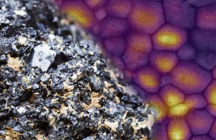
A family of compounds known as perovskites, which can be made into thin films with many promising electronic and optical properties, has been a hot research topic in recent years. But although these materials could potentially be highly useful in applications such as solar cells, some limitations still hamper their efficiency and consistency.
Now, a team of researchers at MIT and elsewhere say they have made significant inroads toward understanding a process for improving perovskites’ performance, by modifying the material using intense light. The new findings are being reported in the journal Nature Communications, in a paper by Samuel Stranks, a researcher at MIT; Vladimir Bulovic, the Fariborz Maseeh (1990) Professor of Emerging Technology and associate dean for innovation; and eight colleagues at other institutions in the U.S. and the U.K. The work is part of a major research effort on perovskite materials being led by Stranks, within MIT’s Organic and Nanostructured Electronics Laboratory.
Tiny defects in perovskite’s crystalline structure can hamper the conversion of light into electricity in a solar cell, but “what we’re finding is that there are some defects that can be healed under light,” says Stranks, who is a Marie Curie Fellow jointly at MIT and Cambridge University in the U.K. The tiny defects, called traps, can cause electrons to recombine with atoms before the electrons can reach a place in the crystal where their motion can be harnessed.
Under intense illumination, the researchers found that iodide ions—atoms stripped of an electron so they carry an electric charge—migrated away from the illuminated region, and in the process apparently swept away most of the defects in that region along with them.
“This is the first time this has been shown,” Stranks says, “where just under illumination, where no [electric or magnetic] field has been applied, we see this ion migration that helps to clean the film. It reduces the defect density.” While the effect had been observed before, this work is the first to show that the improvement was caused by the ions moving as a result of the illumination.
This work is focused on particular types of the material, known as organic-inorganic metal halide perovskites, which are considered promising for applications including solar cells, light-emitting diodes (LEDs), lasers, and light detectors. They excel in a property called the photoluminescence quantum efficiency, which is key to maximizing the efficiency of solar cells. But in practice, the performance of different batches of these materials, or even different spots on the same film, has been highly variable and unpredictable. The new work was aimed at figuring out what caused these discrepancies and how to reduce or eliminate them.
Stranks explains that “the ultimate aim is to make defect-free films,” and the resulting improvements in efficiency could also be useful for applications in light emission as well as light capture.
Previous work reducing defects in thin-film perovskite materials has focused on electrical or chemical treatments, but “we find we can do the same with light,” Stranks says. One advantage of that is that the same technique used to improve the material’s properties can at the same time be used as a sensitive probe to observe and better understand the behavior of these promising materials.
Another advantage of this light-based processing is it doesn’t require anything to come in physical contact with the film being treated—for example, there is no need to attach electrical contacts or to bathe the material in a chemical solution. Instead, the treatment can simply be applied by turning on the source of illumination. The process, which they call photo-induced cleaning, could be “a way forward” for the development of useful perovskite-based devices, Stranks says.
The effects of the illumination tend to diminish over time, Stranks says, so “the challenge now is to maintain the effect” long enough to make it practical. Some forms of perovskites are already “looking to be commercialized by next year,” he says, and this research “raises questions that need to be addressed, but it also shows there are ways to address” the phenomena that have been limiting this material’s performance.
Source: Phys.org


Leave a Comment
You must be logged in to post a comment.